![[Color Line]](colrline.gif)
For many years I've wanted a 68k system of my own so that I could learn 68k assembler, and be able to work with a processor that has a large address space, i.e. a non-segmented architecture. When 68k microprocessors were so popular, I was unable to afford the thousands of dollars required to purchase one. So, now I'm working on building one, on a plugboard. Once I get it working as intended, I will try to lay out a PCB of the design. Most of the descriptions of small 68k computers that I've seen use smaller memories. I wanted to try to incorporate better hardware than most of them use. Also, it is easy to see that some sort of programmable logic would reduce chip count, in some cases, drastically. And, surface mount technology would greatly reduce the space required to lay out a PCB. That's fine, but I wanted to keep this project as simple as possible, so I'm going to use standard TTL, and through-hole parts. As I am writing this, half-megabyte SRAM in PDIP is available for about $6 a chip from domestic suppliers, and even a little cheaper overseas. So, it ought to be nice to make a 68k with one, or two, megabytes of memory.
It isn't easy to bring up a complex processor, such as the 68K, for the first time. It is especially frustrating when the assembly language is unfamiliar. It gets difficult to distinguish hardware problems from bone-headed assembler mistakes (and there are multitudes of traps in 68K assembler for a newbie (like me) to fall into!). What is it that they say? That chances are that a bug will be found in just 10-12 lines of assembly code? But the effort is well worth it. The 68K is a very nice processor, and 68K assembly is very flexible. I had designed, and built, a number of 8-bit processors in the past before working with the 68K, so I'm not a newcomer to assembler and building computers with chips and wire. But, it was still quite an effort.
The following is the process that I used. It is a staged approach. There are many ways to do it, and this might not be the best way for everybody, but it worked well for me. Please note that I didn't try to include the infamous "free run" step.
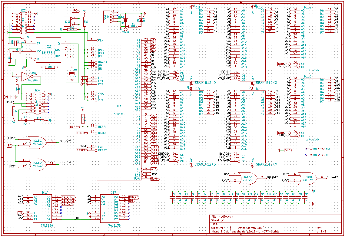
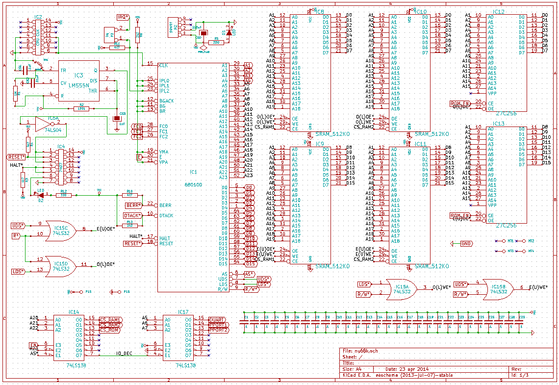
The first step was to build the 68K core, with the processor and only EPROM (at address $0). Of course, that requires a CPU clock (I used an oscillator), the reset circuit, the LS32 to generate EPROM output enable (OE*), and an LS138 to decode addresses and generate chip selects. I used two LS138s because eventually I want to devote an entire LS138 to the I/O devices. I also used an LS367 to buffer the three FC outputs from the CPU to LEDs. They are often useful in trying to understand what the CPU is doing, particularly in the early stages of the build.
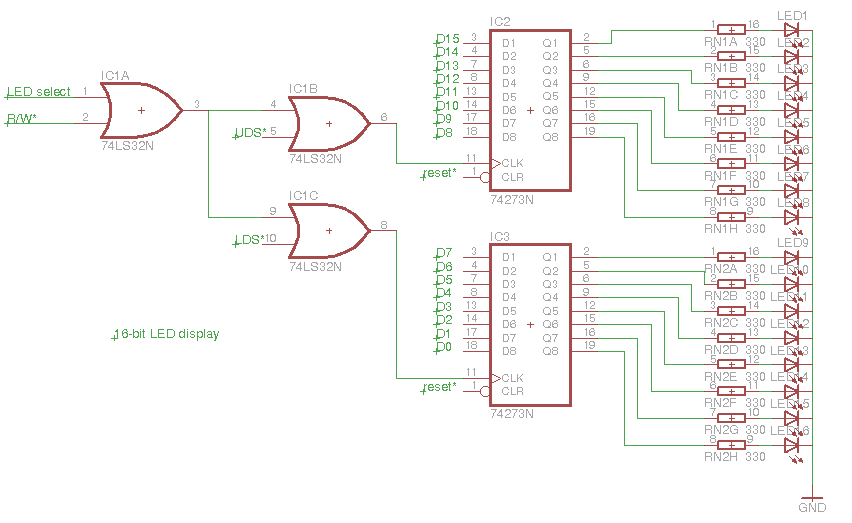
I added a temporary 16-bit LED display for debug purposes. Without any sort of text output, in the initial stages, it seems to me that this is the easiest way to figure out what is going on. It will be removed later on when a DUART, or ACIA, is added. It is quite simple, based on a couple of 74LS273s. It occupies, for the time being, the same addresses that the system console will eventually use ($700000).
The other thing that is critical at this point is grounding DTACK*. I think that removing as many variables as possible will make the task easier. Keep it simple. If a DTACK* generator, for wait states, is desired, it can easily be added later. Grounding DTACK* means that all the memory components must be fast enough for the CPU clock that you are using. I started off with a 4 MHz oscillator, but the memories I was using were capable of much higher speeds (theoretically about 18 MHz, but maybe more realistically 12 or 16 MHz?). That will come later on. The 27C256 EPROMs are 55 n.s. parts.
So, this is the little piece of code I used at this point to test the processor. Whatever is used to check that the processor is working must avoid any use of R/W memory for now, because there is NONE! That means no stack, subroutine calls, etc.
Once that is working, the next step is to add R/W memory. I used 512 x 8 SRAM, again these are 55 n.s. parts. I added them above the EPROM in the memory map. So, for now on my processor, EPROM is $0 to $FFFF, and SRAM is $100000 to $1FFFFF. Of course, since I am not attempting to decode memory addresses below A19 of the CPU, the EPROM image is repeated many times in between the addresses $FFFF and $100000, but that wasn't of much importance to what I did. So, that means that there are 64k bytes of EPROM and 1m bytes of SRAM. There isn't much additional support circuitry required. The other half of the 74LS32 used to generate EPROM OE* is used to generate the write (WE*) signals for the SRAM.
Then I used this piece of code to assure myself that the EPROM was still functional, and to poke around in the SRAM to see if everything was wired correctly there. It starts out by flashing alternate bytes of the 16-bit LED display for a short period of time, and then it writes to, and reads back from, all locations of SRAM to be sure that it is functioning properly. If that is OK, it will go back to start the process all over, and you will see the alternating bytes of the LED display begin to flash again. If there is an error at any location in SRAM, it will light up all the LEDs for a period of time, and then start the process all over again.
Here is the first big trap that I fell into. Writing, and then reading, memory is NO guarantee that it is working correctly. If the "write" circuitry is not working, a "read" can easily produce the same value, making it look like everything is working correctly. The above "test" seemed to indicate that the SRAM was working correctly, but I was to find out (later) that it was NOT.
All of that checked out fine, so I moved on to the next step, which is critical (IMO) to building a useful 68K system. At RESET*, the 68K picks up its stack pointer and initial starting address for execution (the so-called "reset vector") from memory locations $0 and $4 respectively. They are both longwords. Obviously, in order to do this a functional 68K must have some sort of non-volatile memory at those locations when the CPU is reset. It is possible to leave the memory map with the EPROM at location $0, but that detracts from the flexibility of the system. There are lots of 68K applications available (probably because of the Motorola Educational Computer Board that was so popular when the 68K was first introduced?) and they mostly run in R/W memory at addresses less than $1000, or so. Modifying them to run in high memory (where my SRAM is presently located) is fraught with problems, especially for a novice 68K assembler programmer (like me!). I've had my share of "adventures" there! More importantly, if there is interest in getting something like CP/M 68K to run on your system, it must have R/W memory in the lower address space, not EPROM. So, I adapted a method that I had seen in several places to "swap" EPROM and SRAM address space after the reset vector had been picked up at locations $0 and $4. It uses a 74LS164 to disable the SRAM and make the EPROM appear to reside at $0. This happens during the first four (or eight, if you are using a 68008) clicks of AS*. After that, the memory address decoding 74LS138 is enabled, and normal addresses pertain. Once the 74LS138 is enabled, SRAM is found at $0 to $FFFFF, and EPROM at $100000 to $10FFFF.
Besides the 74LS164, a 74LS08 is needed to pull this off. Once that wiring is in place, this piece of code can be used to check that all is well. It is very similar to the last program used, except that the "reset vector" and a number of addresses must be changed. When it is working properly, you are ready to move on to adding some sort of I/O port.
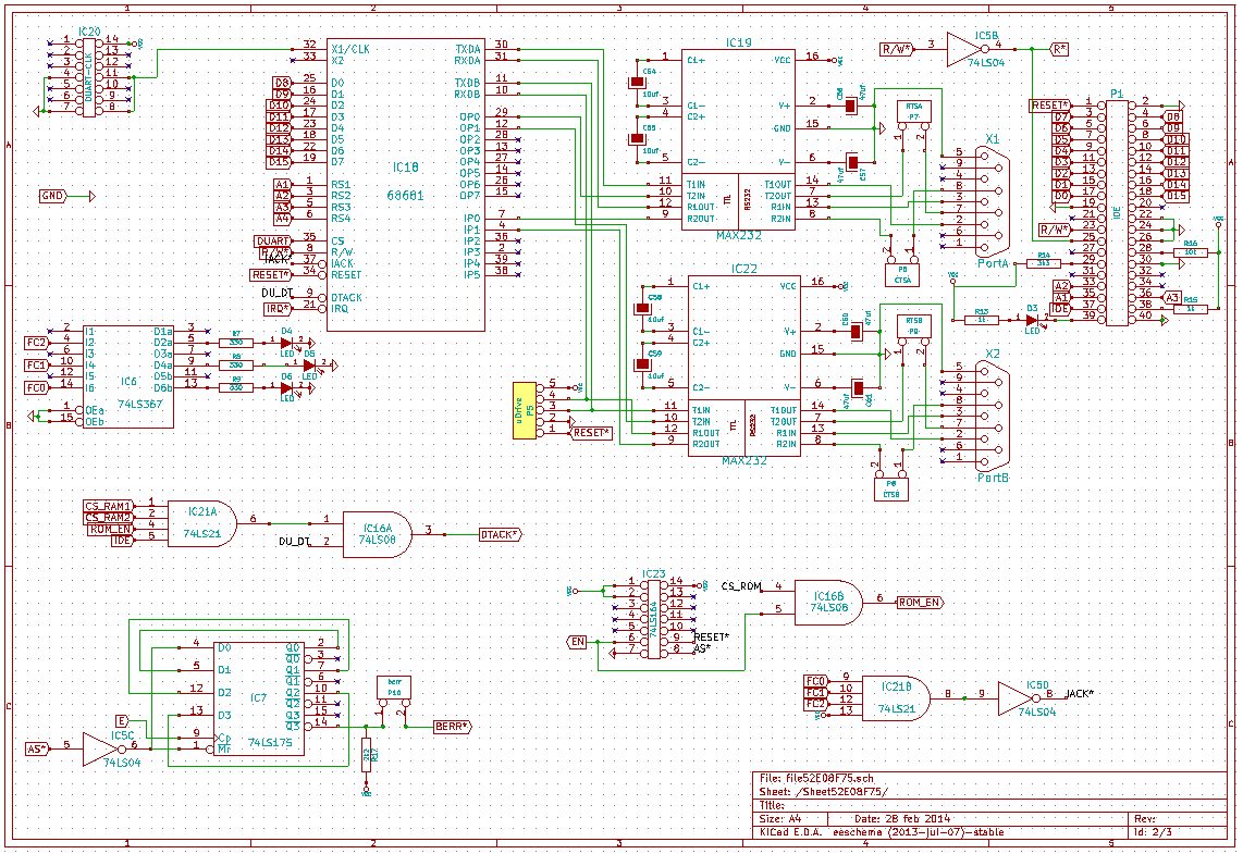
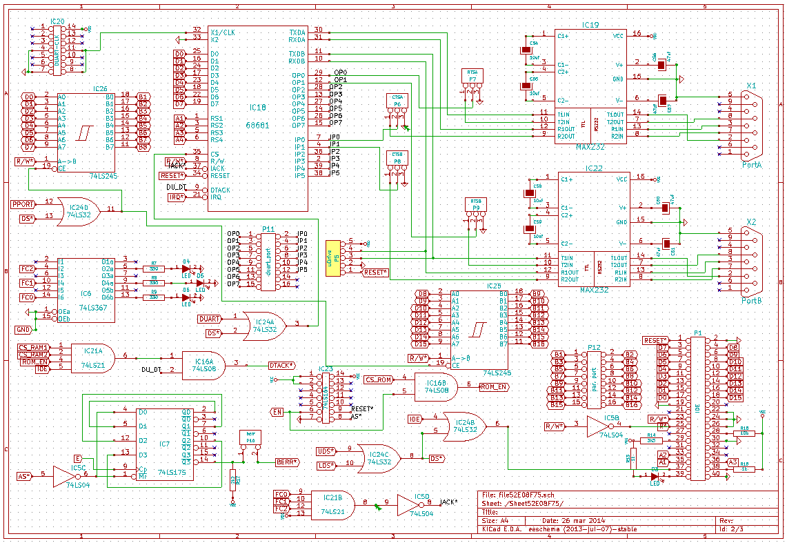
At this point, the system builder must make a decision. There are a number of options available for a system console. Classically, the 6850 ACIA has been used for serial port(s). There is a newer DUART available, the 68681, that is also often used with the 68K. A couple of other choices are available too. There are a number of USB-to-parallel devices based on the FTDI 245 USB to parallel FIFO chip (such as the DLP USB245R, etc.) that might be used to provide a direct connection to USB (without a UART). Also, one of the many, many micro-controllers (PIC, Atmel, etc.) might be used to provide a link between the 68K and a console. A micro-controller co-processor, if you will. I haven't got much to say about those options. I have used both a 6850 ACIA and a 68681 DUART, and got both working. I will provide information about both of them here.
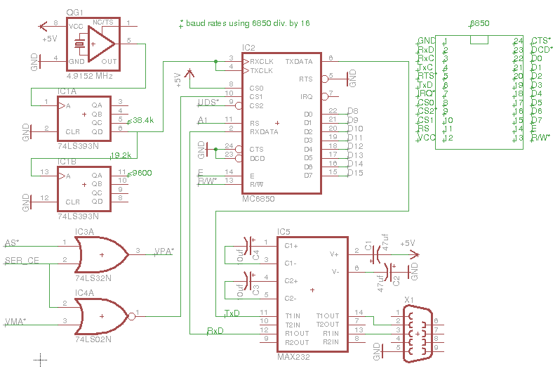
The choice between them is (IMO) a toss-up. The 6850 is old, and has been around for a long time. Most designs using it with a 68K imply that it can only be used to connect at speeds up to 9600 baud. I was able to get the ones that I used to run at 38.4k and 19.2k baud, and I'm now running one at 19.2 reliably. I don't know about long term use of 38.4k baud (yet). I have also used 9600, and it seems to work quite well (not really a suprise!). The 6850 uses the synchronous interface of the 68K. Here is the schematic of the circuit I used. The device is very simple to initialize. On the negative side, there is no RESET* on the chip, but there are a ridiculous number of chip selects (3)! Only one serial port per chip (24-pins). The 68681, on the other hand, is a 40-pin chip with two serial ports. There are also some parallel inputs and outputs on the chip. It is at least capable of 38.4k baud. It has a great deal more flexibility than the 6850 ACIA, but initialization of the chip is far more complex. It bears out the old adage, "the price of function is complexity." I believe that a pair of 6850s would take up a little more board space than one 68681 (including the support circuitry), but probably not much more. The more limited serial baud rates of the 6850 might tip the scales away from it? Perhaps if only one serial port is needed, the 6850 would be the best option? Eventually I want to use a uDrive (see www.4DSystems.com.au on-line), so I will need that second serial port.
In order to add either serial I/O option, it is necessary to abandon the hard-grounded DTACK*, and use some method of providing an active DTACK* signal. In the vein of keeping it simple, I used a 74LS21. Actually, any positive AND gate could be used. That would be the 74LS08, 74LS11, or 74LS21. It all depends on how many devices (how many inputs) need to supply DTACK*. The 68681 has a DTACK* output (the 6850 must not assert DTACK* because it uses the synchronous interface of the 68k), and we have to generate DTACK* for the SRAM and EPROM. Be sure to make provision for any other device you plan to incorporate. I want to add an IDE interface eventually, and another bank (1 more MB) of memory, so a 74LS21 was used. You may cascade a number of positive AND gates to expand the capacity. Since all memory devices I'm using are fast enough for the chosen system clock (4 MHz at first), I just used the chip selects for them as inputs to the AND gate.
At first, I tried to wire in a 68681, but I found that it was difficult to get it working with very little diagnostic capability, so I removed it and put in a 6850. [Remember that I am working with UV erasable ROMs, so having to burn some code, check it, make corrections, erase them and repeat was too time consuming. (I don't have an EPROM emulator!) I went for the 6850 because it is easy to get working. When I have a monitor to provide serial output and allow testing code on-the-fly, I'll go back to getting a 68681 to work.] The 6850 was easy to get working, and I was quickly able to test it with a little "echo" program to read keyboard input and put it back out to the screen. Notice that I wrote it in-line to avoid using any read-write memory (because I thought that it was working, but I wasn't 100% sure). As soon as I converted the exact same code to subroutine calls here, it failed. The "good" write-then-compare test, described above, confused me, and kept me from looking at the obvious for a while. But when I was finally confronted with the fact that R/W memory wasn't working, I checked my wiring more carefully and discovered that WE* for the "upper" SRAM chip was wired wrong. After I fixed that, I used this little diagnostic to check. It uses both the LEDs and the serial port. It pushes a known entity (the letters of the alphabet, one by one) onto the stack, and then pops them back off and displays them. That worked correctly, so I re-tried the "echo" code, written as subroutine calls. It worked!
So now it is time to try to load some sort of monitor. I found a very simple one (following my plan of keeping it simple) in "The 68000 Microprocessor", by James Antonakos. It only has 4 functions (Edit, Dump, Move, and Go) along with "Help". Not much in the way of bells and whistles, but easy to get working. Here is my adaptation, to run in high memory ($100000). It was easy to modify and worked on my first try. And here is a sample of the output. I was also able to poke a tiny "fill" function into R/W memory and run it. It took about 7 seconds to fill 1MB of memory with zeros. This is still with the 4MHz system clock. I'm still learning 68k assembler (there's a lot to learn), so the way I did it is probably not the most efficient way.
With a functional serial port, the LED display was no longer needed, so I removed it.
It is March 2014 now, and there is a lot more to do, both hardware and software. I intend to go back to the 68681, and I'd like to try to get an IDE interface working so that I can use one of the IDE to CF adapters to add a CF "hard drive". At this point, I haven't implemented any of the IRQ, IACK, or BERR circuitry either.
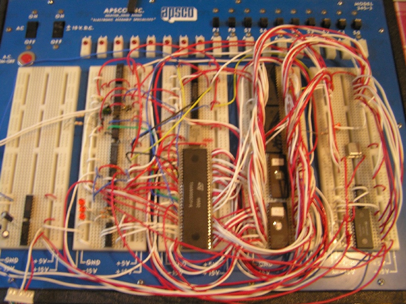
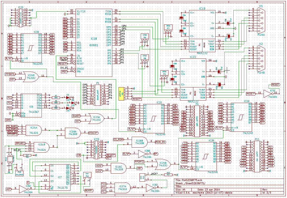
Here is the two-sheet schematic that I've developed A and B, and a photo of the prototype. To the best of my knowledge, the schematic is correct, but in the process of building my system, I have found errors, and I update it to correct them as I go along. BUT, be warned that they may still contain errors, and thus is subject to change.
OK, so it's now nearly the end of March. I've added a 68681 to the prototype, and gotten the "A" port working. After doing that, I pulled the 6850 out of the plugboard in order to make more room for what will follow. The 68681 was a struggle for me, and I still haven't gotten the "B" port working. This is with polled I/O only. I haven't taken the time to experiment with interrupts yet. I also upgraded from the 4 MHz system clock to 8 MHz. So now with that change, and running 38.4k baud to the console, the 68k is quite responsive.
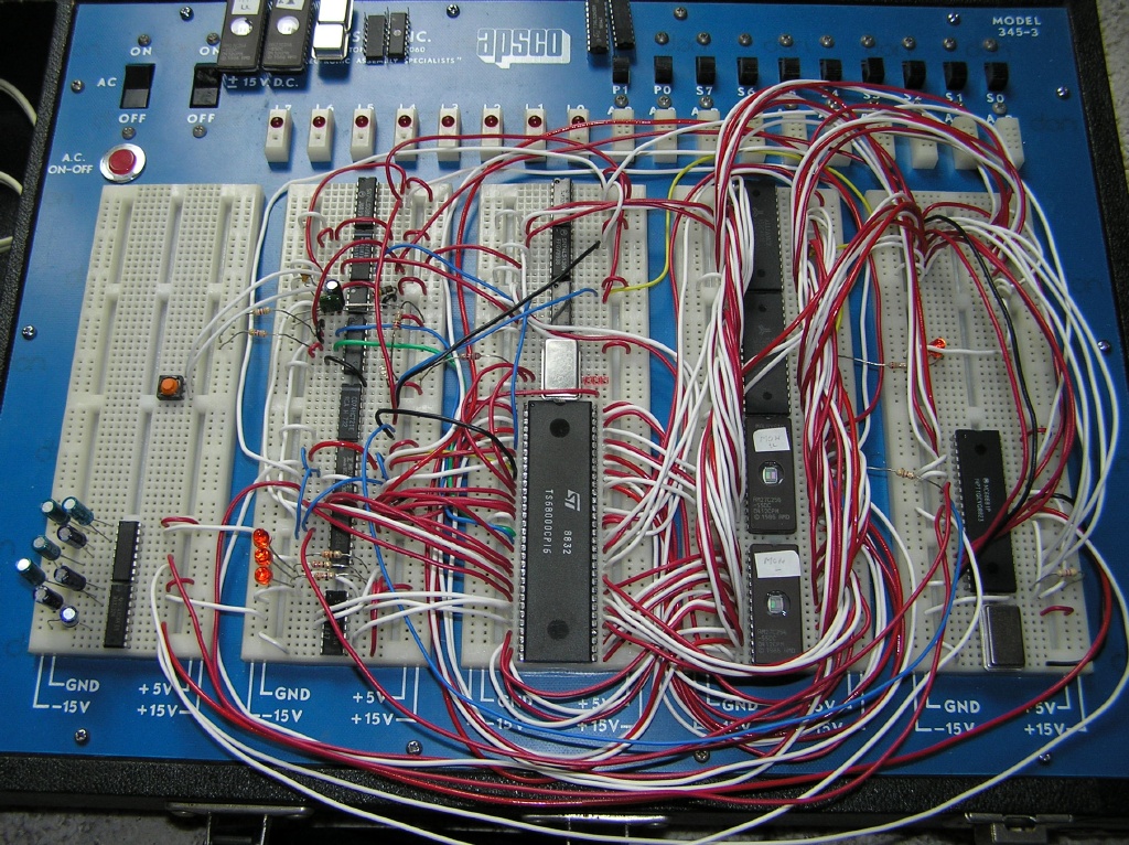
Here is a photo of the project, and here are the two schematics, A and B updated with what is running so far, as well as a few things that I want to add next. I've also added some functions to the monitor. The "load" function is quite handy for reading S-records into memory. I was able to load a version of Tiny Basic for the 68k with it, and run a few simple BASIC programs. I could do the same with the FIG FORTH for the 68k. I'm not much of a FORTH programmer, so I wasn't able to give FORTH much of a test, but it seems to work OK.
OK, so it's now the middle of April. I've had quite an "adventure" with the compact flash interface, and sadly, it does not work. I've tried many, many things, and I was able to get the compact flash (actually several different brands and capacities) to respond to a "get ID" command, and even a "read sector" command. BUT, I've never been able to get a "write sector" command to work. I'm giving up on it, at least trying to get it to function on the raw 68k bus. Maybe it would work with some sort of a PIA in between it and the CPU?? Don't know. I'm looking at a number of options, including SD. The mass storage issue is still up in the air.
While working on this, I discovered a greatly enhanced version of the Antonakos monitor, with a number of very useful functions added. The assembly listing is here. This version has a disassembly function, breakpoints, and trace capability. I find the trace a great way to debug code, and watch what happens to registers as it executes. I've even tweaked the monitor a bit with some features of my own. There are a few things I don't like about it, but I've not taken the time (yet) to try to "fix" them. For example, the display function doesn't operate the way I'd like it to. You specify the starting address as the first argument, and the number of lines (16 bytes per line) as the second, instead of merely giving an ending address. It also makes a big deal of the supervisor bit being set. I can't understand that. What possible difference can it make to run as supervisor on a single user SBC??? Makes no sense. I've tried to correct that situation, but I'm not sure that what I've done makes any difference. In the routine TRACE4, the SR supervisor bit was getting masked off. I changed that. The "GO" command seems to do strange things when there are no breakpoints set, so I added a "JUMP" command that just jumps to the address specified as the first argument. It is particularly inelegant because there is no provision made for returning to the monitor. That is entirely up to the user. The "LOAD" command displayed the S-records on the screen as they are received. I found my 68k too slow (still 8 MHz) to handle that during the real-time load operation, so I killed that display, and instead, I display the S-records on the sender's side. Plenty of excess speed there! Oh, and it seems that a "LOAD" operation will not work correctly twice in a row, without a hard reset. I haven't had the time to look into that yet. All in all, however, I find this monitor a great improvement over what I had been using.
It is now the middle of May. There have been lots of changes. I decided to try to implement an IDE interface via an 8255, but I was running out of room on my plugboard. I rigged up a temporary add-on to my plugboard that serves as the 8255 interface. I have been able to read and write a sector to a compact flash, and get the CF to cough up ID info. All of this using an IDE to CF adapter that can be purchased for not much money. I'm now working on an "exerciser" to drive the CF in a more efficient manner. It is a big project.
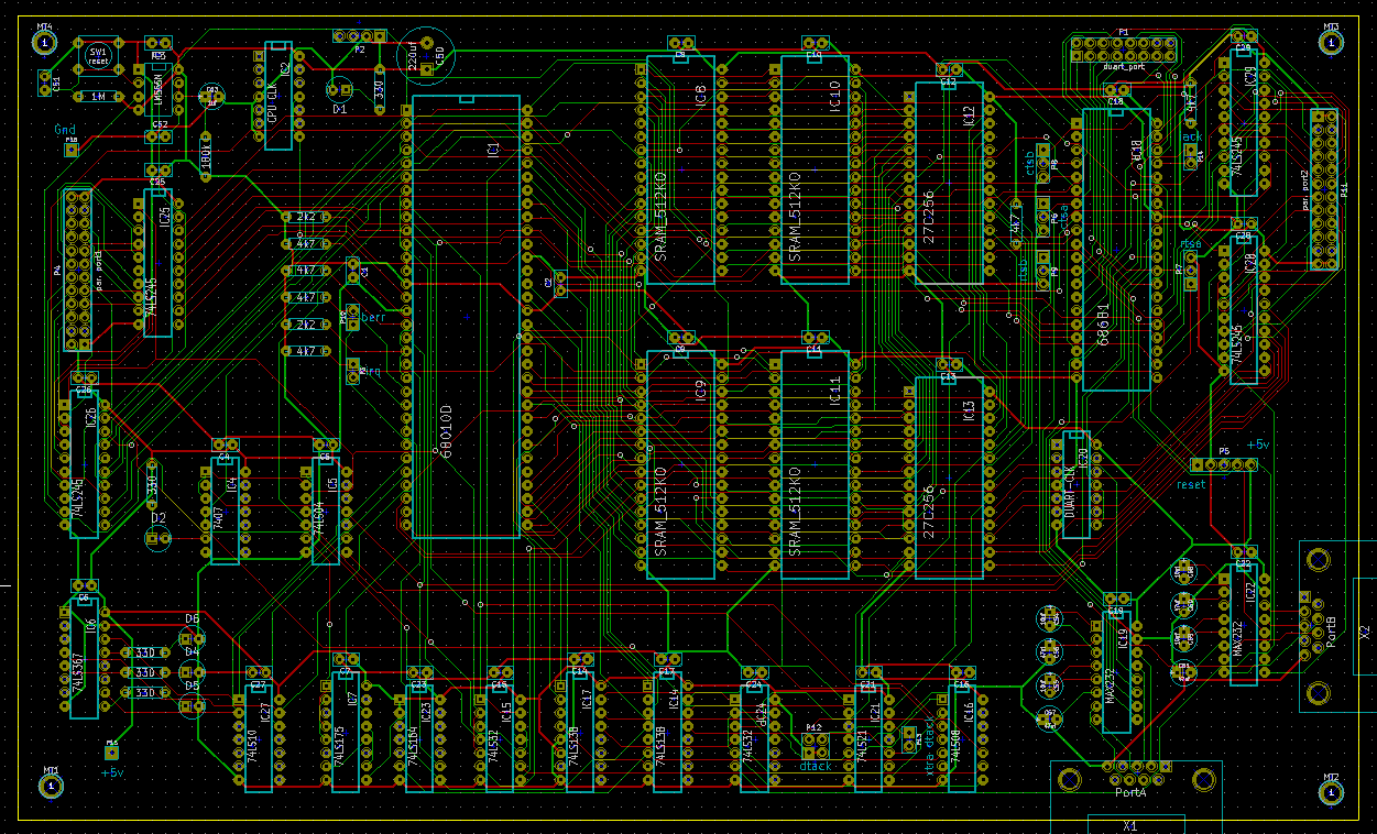
When I realized that the plugboard is nearly max-ed out (space-wise), I started to think about fabricating a PCB to move the parts of the 68k prototype, that had been tested and proven functional, off of the plugboard to make more room for the things that I am still working on. So, I worked up a PCB lay-out and sent it to be fabricated. I've gotten it back, and built up one. It has 2m bytes of SRAM, but still 64k bytes of UV erasable ROM. The RAM is at addresses $0 to $1FFFFF. The ROM is at $200000 to $20FFFF. A 68681 DUART is used at $700000, and there are two 16-bit parallel ports (based on 74LS245s) at $700020 and $700040. I added a circuit to catch bus errors, and tried to make provision for interrupts from the DUART. I wish I had more experience with interrupts on the 68k, but I don't. What I did is probably insufficient. On a single-user SBC, there isn't much need for a complex interrupt structure, so I didn't even use a 74LS148 priority encoder. The DUART interrupt is wired as priority 4 (IPL2*), but I don't know if that is practical.
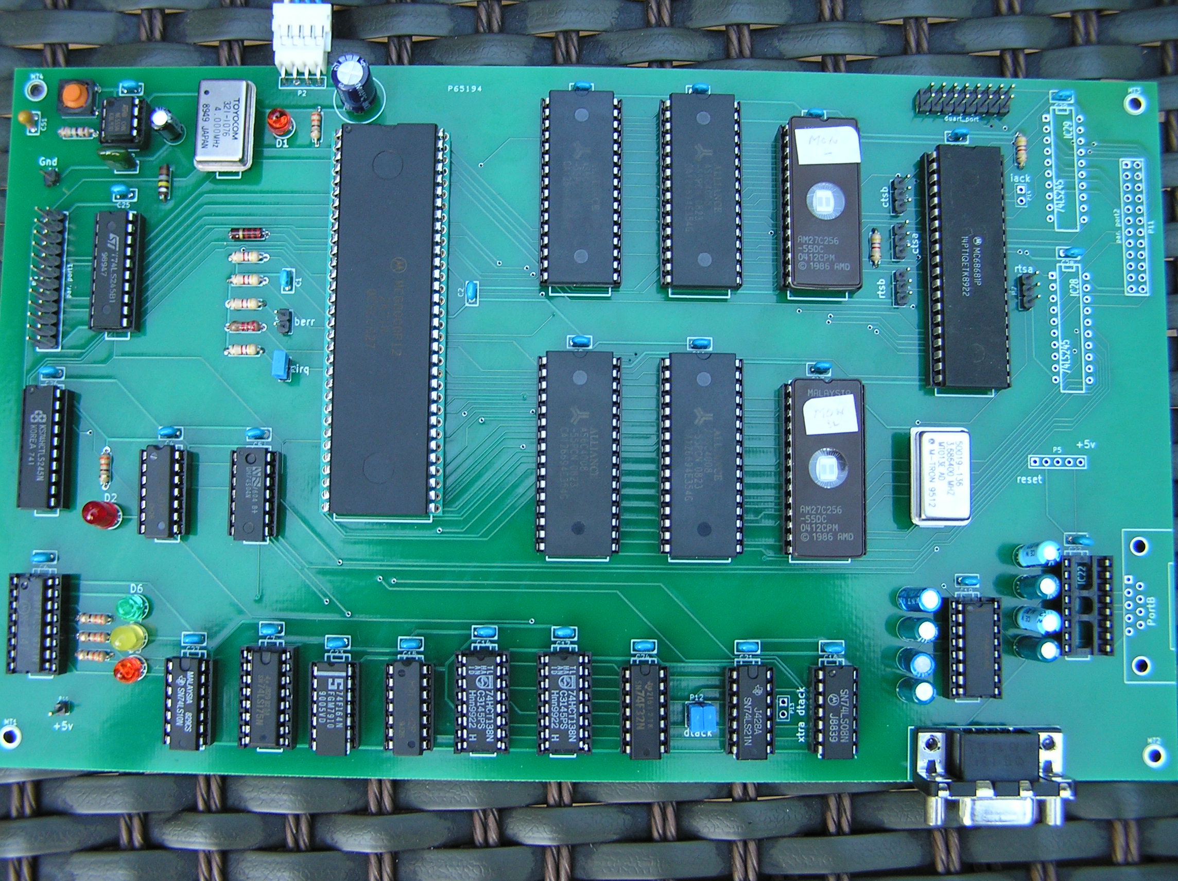
Anyway, here are the schematics for the PCB: sheet A and sheet B. This is the printed circuit board, and see a photo of it here. So far, I haven't found any real errors in the PCB. I wanted the power connector to be compatible with the mini-floppy connector on a PC power supply, but I got it backwards. I had to make a little jig to convert the power connection. Also, I used a single 2.2k pull-up resistor to pull-up the unused pins of the 68k (BG*, BGACK*, BR*, VMA*, VPA*, etc.), and I had a little problem with that. I think I should have used a 2.2k SIP to put a single pull-up resistor on each of these pins. That's all I've found to date.
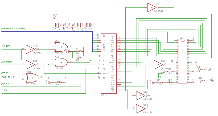
After more testing, the PCB seems quite solid. It is running at 10 MHz. I have been working with an IDE-CF interface based on the 82c55, and I've gotten it working quite well. I have a little application, that is menu driven, that can be used to read and write sectors, and retrieve the CF i.d. information. I've transferred the circuit I used to a little schematic. Parts of it may be over engineered, but it is a snapshot of what seems to work well. I'll be continuing to improve it, with the goal in mind of making some sort of mass storage device that can be used (eventually) as a disk drive for a real operating system. Take a look at the schematic here. Note that the schematic does not include any means of generating DTACK* for the 82c55. You are on your own for that.
It is now early June. I've been able to move the IDE-CF interface over to the 68k PCB, and it seems to work OK. Please note that I had to make a few changes to the schematic (link above). Most have to do with generating 82c55 RD* and WR*. I'm still checking it out, but if everything is stable, I'll be moving on to work on being able to boot some sort of operating system from CF.
July is two thirds gone now (2014), and the 68k project is progressing. I have refined the compact flash access quite a bit. It seems to work very reliably for the 4 GB Kingston module that I'm using (the one with the picture of a pinkish-white flower on it). I've found that the newer the CF is, the better it works. I have 16, 32, 128, 256, and 512 MB models, as well as 1, 2, and 4 GB ones. The 16 and 32 MB compact flash modules are sort of flakey. All the others work much better.
I've been able to load the CP/M 68k (v. 1.3) image (CCP and BDOS) that was copied from the original Digital Research distribution diskettes. There are two versions given in S-record form, one that loads at $400, and one that loads at $15000. I used the one that loads at $15000. I wrote a do-nothing CBIOS to go with the image, and I can get the "A>" prompt. There is no disk read/write code in this CBIOS yet, so there isn't much that can be done with it in the way of meaningful testing. The bad news is that this code consistently generates an error message about a "$03 exception" (I'm assuming that's an address exception). The memory address given is inside the Digital Research code. It seems that CP/M 68k, when it runs, takes over a good deal of the 68k exception table (via the "setexc" system call). I don't know what to do about this error message yet. I'm going to continue to work on adding disk I/O capability to the CBIOS, and see if that eliminates the message. At first, I will implement a CBIOS without any block/deblock code. That will waste three fourths of the storage capacity of the compact flash (only put data in the first 128 bytes of each 512 byte compact flash sector). If I can get that working, I'll try to add in block/deblock code later.
I'll post the CBIOS code I'm using at a later date, as soon as I can clean it up some.
As always, this is a work in progress. I hope to update this site when there is progress to report. And the schematics are always changing as I find errors and omissions.
I'd love to hear from anybody who has similar interests, and who might want to contribute ideas or participate in fabricating a final PCB.